

Engineers at the University of California, Berkeley, are reporting a new way of creating computer chips that could revitalize optical lithography, a patterning technique that dominates modern integrated circuits manufacturing.
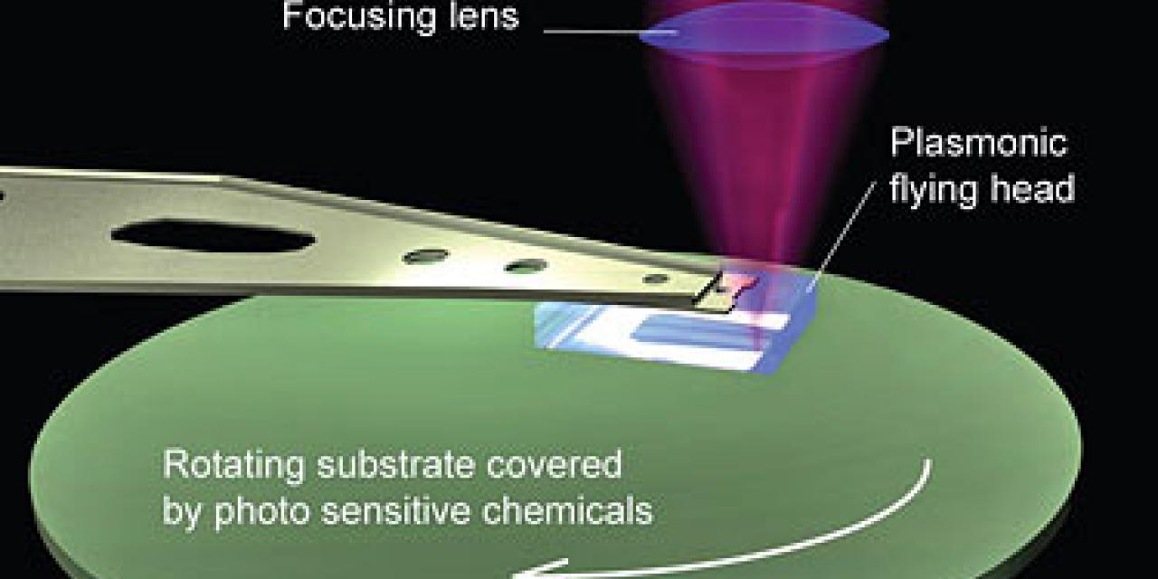
By combining metal lenses that focus light through the excitation of electrons - or plasmons - on the lens' surface with a "flying head" that resembles the stylus on the arm of an old-fashioned LP turntable and is similar to those used in hard disk drives, the researchers were able to create line patterns only 80 nanometers wide at speeds up to 12 meters per second, with the potential for higher resolution detail in the near future.
"Utilizing this plasmonic nanolithography, we will be able to make current microprocessors more than 10 times smaller, but far more powerful," said Xiang Zhang, UC Berkeley professor of mechanical engineering and head of the research team behind this development. "This technology could also lead to ultra-high density disks that can hold 10 to 100 times more data than disks today."
Zhang worked jointly on the project with David Bogy, UC Berkeley professor of mechanical engineering. The study now appears online in Nature Nanotechnology, and is scheduled for the journal's December print issue.
The process of optical lithography shares some of the same principles as film photography, which creates pictures by exposing film in a camera to light, and then developing the film with chemical solutions. In the semiconductor industry, optical lithography is a process in which light is transferred through a mask with the desired circuit pattern onto a photosensitive material, or photoresist, that reacts chemically when exposed. The material then goes through a series of chemical baths to etch the circuit design onto a wafer.
"With optical lithography, or photolithography, you can instantly project a complex circuit design onto a silicon wafer," said Liang Pan, a UC Berkeley graduate student working with Zhang and Bogy, and one of three co-lead authors of the Nature Nanotechnology paper. "However, the resolution possible with this technique is limited by the fundamental nature of light. To get a smaller feature size, you must use shorter and shorter light wavelengths, which dramatically increases the cost of manufacturing. Also, light has a diffraction limit restricting how small it can be focused. Currently, the minimum feature size with conventional photolithography is about 35 nanometers, but our technique is capable of a much higher resolution at a relatively low cost."
The UC Berkeley researchers chose a different approach to overcome the diffraction limit of light. They took advantage of a well-known property of metals: the presence at the surface of free electrons that oscillate when exposed to light. These oscillations, which absorb and generate light, are known as evanescent waves and are much smaller than the wavelength of light.
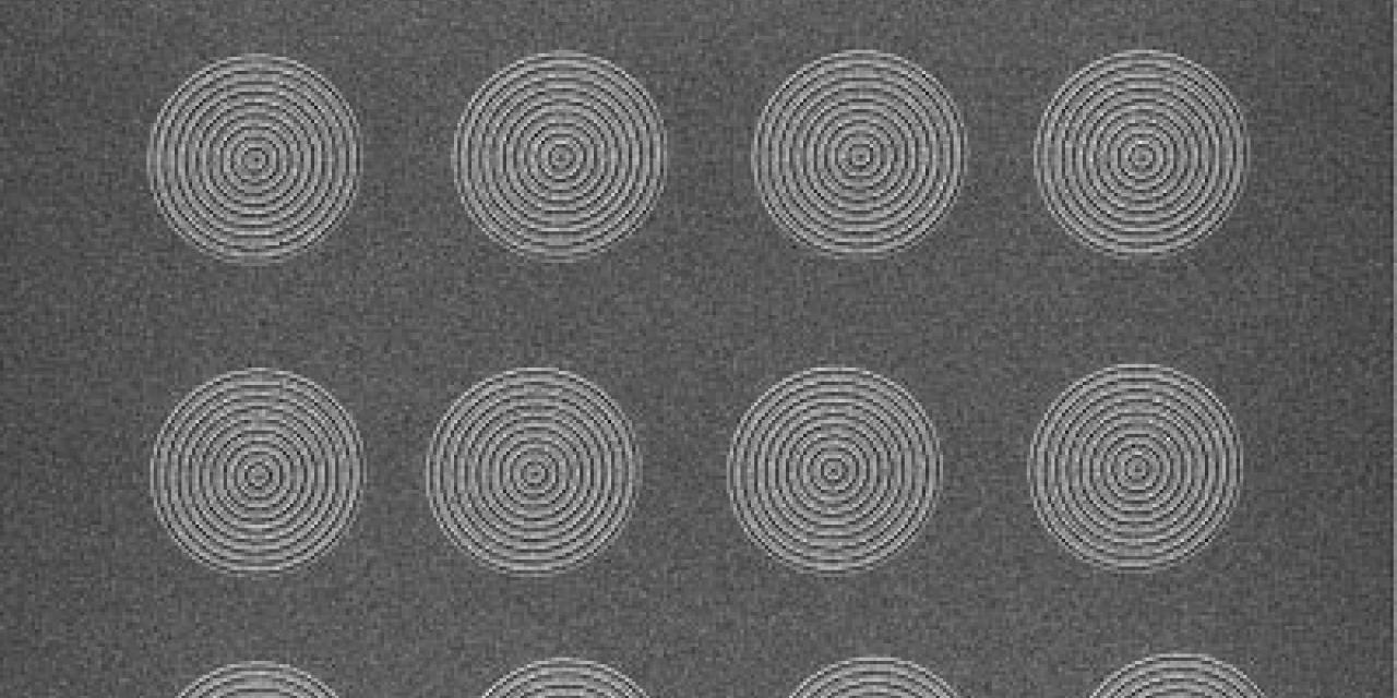
The engineers designed a silver plasmonic lens with concentric rings that concentrate the light to a hole in the center where it exits on the other side. In the experiment, the hole was less than 100 nanometers in diameter, but it can theoretically be as small as 5 to 10 nanometers. The researchers packed the lenses into a flying plasmonic head, so-called because it would "fly" above the photoresist surface during the lithography process.
Similar flying heads have been developed at UC Berkeley's Computer Mechanics Laboratory, which is directed by Bogy. "Flying heads support the phenomenal advances in data storage in hard disk drives," said Bogy. "They enable the fast speeds and nanometer accuracy required in this potentially new approach to semiconductor manufacturing."
The researchers said the flying head design could potentially hold as many as 100,000 lenses, enabling parallel writing for even faster production.
The researchers compared this flying plasmonic head to the arm and stylus of an LP turntable, with the photoresist surface spinning like a record. Instead of a needle moving along the grooves of a spinning record, however, the flying plasmonic head contains a nanometer-scale optical stylus that "writes" onto the spinning surface of the photoresist without actually touching it.
Because the light from plasmons decays less than 100 nanometers from the metal surface, the photoresist material must be placed very close to the lens. To accommodate this limitation, the researchers designed an air bearing that uses the aerodynamic lift force created by the spinning to help keep the two surfaces a mere 20 nanometers apart.
Air bearings are used to create magnetic tapes and disk drives, but this is the first application for a plasmonic lens.
With this innovative setup, the engineers demonstrated scanning speeds of 4 to 12 meters per second.
"The speed and distances we're talking about here are equivalent to a Boeing 747 flying 2 millimeters above the ground," added Zhang. "Moreover, this distance is kept constant, even when the surface is not perfectly flat."
The researchers pointed out that a typical photolithography tool used for chip manufacturing costs $20 million, and a set of lithography masks can run $1 million. One of the reasons for the great expense is the use of shorter light wavelengths to create higher resolution circuitry. Shorter wavelengths require nontraditional and costly mirrors and lenses.
The system described by the UC Berkeley engineers uses surface plasmons that have much shorter wavelengths than light, yet are excitable by typical ultraviolet light sources with much longer wavelengths. The researchers estimate that a lithography tool based upon their design could be developed at a small fraction of the cost of current lithography tools.
Other alternatives have been developed that can achieve higher resolution than conventional photolithography and without the need for a lithography mask. However, those techniques - electron beam lithography, scanning probe lithography and focused ion-beam lithography - work at a snail's pace compared to the flying plasmonic lens system, said the UC Berkeley researchers.
Zhang noted that the flying head design is not limited to plasmonic lenses. His lab has been developing metamaterials - composite materials capable of bending electromagnetic waves in extraordinary ways - into lenses that can be used for nano-optic imaging and other applications.
"I expect in three to five years we could see industrial implementation of this technology," said Zhang. "This could be used in microelectronics manufacturing or for optical data storage and provide resolution that is 10 to 20 times higher than current blu-ray technology."
The other co-lead authors of the study are Werayut Srituravanich, a former Ph.D. student in Zhang's lab and currently a lecturer in mechanical engineering at Chulalongkorn University in Thailand, and Yuan Wang, a UC Berkeley graduate student in mechanical engineering. The study was also co-authored by Cheng Sun, a former graduate student in Zhang's lab and currently an assistant professor in mechanical engineering at Northwestern University.
This work was supported by the National Science Foundation Center for Scalable and Integrated Nano-Manufacturing.


