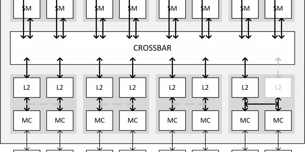
NVIDIA has confirmed and explained the GeForce GTX 970 design flow that makes the last 512 MB of the card's VRAM incredibly slow.
The explanation, along with a neat architecture diagram, was provided by NVIDIA’s Senior VP of GPU Engineering, Jonah Alben. We already know that GTX 970 is basically a downgraded version of the reference GTX 980 GPU. Alben explained that the main differences between the two cards include disabling 3 Streaming Processors (SM) from the GTX 980's 16 SM's and disabling one block of its 8 blocks of level 2 cache.
Each SM includes 128 CUDA cores, so 13 SM's sum up to the 1664 CUDA cores specified by NVIDIA in the card's manual. However, having only 7 blocks of L2 cache means that the GTX 970 has only 1792 KB of L2 cache, which is 12.5% less than the 2048 KB figure reported by NVIDIA to hardware reviewers. Alben acknowledged the misinformation and brushed it up to a "misunderstanding between the engineering team and the technical PR team."
To be fair, the GeForce GTX 970 L2 cache size is not mentioned in the hardware specifications released to the general public.
To fully understand the VRAM speed problem at hand, we have to go into more technical details of NVIDIA's Maxwell architecture. The reference Maxwell architecture divides its 4GB VRAM into 8 512MB VRAM blocks, each controlled by one L2/MC unit. In order to maximize speed, every piece of data written to the VRAM is split into 8 parts that are sent to the 8 L2/MC units to be written simultaneously. But in the GTX 970, the 7th L2/MC unit is actually responsible for 2 VRAM blocks which means that it takes twice as much as the other units to write, leaving them idle for 50% of the time.
To fix this problem, NVIDIA divided the GeForce GTX 970 memory to two pools: a 3.5 GB pool and a 0.5 GB one. The first pool is controlled by 7 L2/MC units working in parallel and hence it operates at full speed while the second pool is controlled by a single L2/MC unit which means that its access speed is one seventh of that of the larger pool.
The above explanation provided by Alben certainly agrees with the benchmark results which showed that the last 0.5 GB of GeForce GTX 970 VRAM is accessed at 20 GB/s while the rest of the card's memory is accessed at 150 GB/s.
But Alben insists that this performance impact can be witnessed only in synthetic benchmarks and it has little to no impact in real gaming scenarios. He argued that the memory pools are designed so that the operating system would be fully aware of their speed differences and hence the slower 0.5GB VRAM pool is used to store infrequently accessed data only.
According to NVIDIA's performance labs, the performance hit of the GeForce GTX 970's slower memory pool is in the 4% to 6% range in real games.


