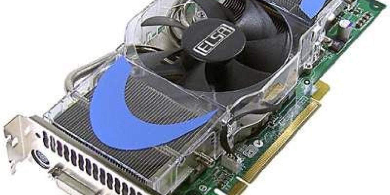

Earlier today some information regarding the possible specs of nVidia's upcoming G80 based boards surfaced on VR-Zone, only to be "quietly" removed later. Thankfully X-bit labs managed to collect the information on the new cards and we can now present it to you below.
The most important aspect of the leaked documentation are the specs revealed:
- Unified Shader Architecture;
- Support FP16 HDR+MSAA;
- Support GDDR4 memories;
- Close to 700M transistors (G71 - 278M / G70 - 302M);
- New AA mode: VCAA;
- Core clock scalable up to 1.5GHz;
- Shader performance: 2x Pixel/12x Vertex over G71;
- 8 TCPs & 128 stream processors;
- Much more efficient than traditional architecture;
- 384-bit memory interface (256-bit+128-bit);
- 768MB memory size (512MB+256MB)
The unified shader architecture suggests, what the experts have been saying for a while now, that the cards will be support DX10.
According to the same, leaked, information the G80 will surface in November in two varieties, the GeForce 8800 GTX and GeForce 8800 GT priced at a mere USD 649 and USD 449-499 respectively. The GTX model (higher-end) will feature a 384-bit memory interface, a hybrid water and air cooler and 7 TCPs while the GT will have a 320-bit memory interface, a standard air cooler, and 6 TCPs.
No one has actually explained what TCP actually stands for although Techreport has uncovered an nVidia patent which refers to thread control processors. According to the same patent these TCPs will be used to set the function of the unified shader processors.
